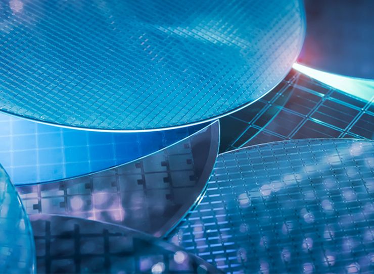
Glass Wafer
The need for low-cost miniaturization has driven Wafer Level Packaging to evolve from the semiconductor industry and adapt to emerging technologies in a wide array of markets. As this manufacturing process has evolved, so too has Coresix, growing into a world leading producer of Glass Wafers.
Coresix has walked the path from development to volume production to next generation with many of our valued customers. Whether you need help developing your wafer specifications, or you need a supplier who can meet your most demanding specifications, Coresix is experienced in all aspects of wafer manufacturing.
PROCESS
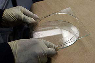
Shape Cutting
The introduction of materials into the glass wafer fabrication process usually involves the sizing of the substrate for subsequent operations. This can be achieved by several means depending on the overall diameter, thickness, and type of glass being used. Thin sheets are scribed, thick sheets are water jetted and blocks are wire sewn to begin the process with a wafer blank.

Edging
At Coresix, we have the capability to apply the most effective edge solution for every application including 45°, radius, radius blend, and custom edge profiles. Each clear glass wafer is individually edged on a Precision CNC Edge Grinding Station. Where required, physical features are applied including Semi Standard Flats and Notches, alignment marks, cavities, and holes.
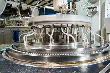
Lapping
For glass wafer applications requiring characteristics not available in the raw glass including thickness, thickness tolerance, thickness variation, flatness, and parallelism, these critical specifications are established early in the fabrication process through double-side lapping. We run multiple platforms and variations of the lapping process to consistently meet the most stringent of these requirements from small volume R&D to high volume production.
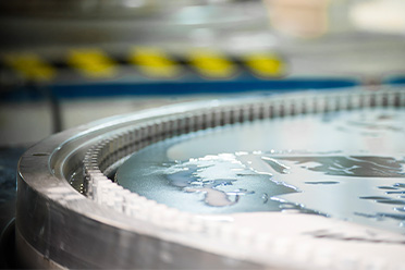
Polishing
Once the physical characteristics of the glass wafer have been achieved through double-side lapping, our polishing processes focus on creating clear, pristine surfaces. Coresix has the capacity to run high volumes of glass wafers through various double-side polishing processes including Commercial Polish to remove subsurface damage, final polish to create flawless surface finishes, and Super Polish to achieve smooth surfaces to 2Å RMS

Laser Marking
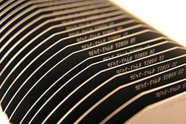
Coresix has multiple UV and CO2 laser systems for the application of unique serialization to glass wafers. Our systems accommodate SEMI standards and custom parameters to the precise location. Once the laser mark is applied, the glass wafer is re-cleaned and inspected before final packaging. Wafer IDs can be applied to the label and data provided to each part.
Cleaning
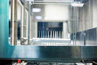
Our ability to deliver glass wafers in a clean, residue, and particle-free condition is unique and unsurpassed in the glass wafer market. We combine ultrasonic and mega-sonic on multiple cleaning lines which feed directly into a Class 100 Optical Clean Room where we inspect various quality levels under the appropriate lighting conditions.

Inspection
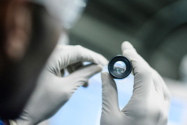
A surface imperfection not visible to the naked eye can become a glaring defect when magnified in the end product. A particle of glass, a fingerprint, a water spot may go unnoticed until enhanced by the application of optical films. In our Optical Clean Room, under established lighting conditions, our experienced inspectors detect particles and defects to sub-micron levels.
Packaging
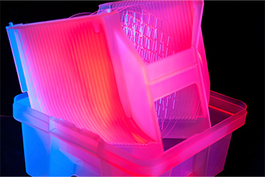
Standard format glass wafers are packed in pre-cleaned, semiconductor wafer containers double bagged and vacuum-sealed within the Class 100 Optical Clean Room. Ultra-thin or non-standard format wafers are alternatively packed in coin stack jars or custom containers for worldwide shipment in high volume. Custom wafer pallet systems assure safe delivery while minimizing transportation costs.
SPECIFICATION
Dimensional Specifications
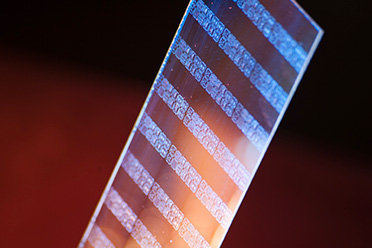
Coresix produces wafers to all SEMI Standards including dimensional, flat and notch specifications. In addition, we offer custom specifications designed to your unique needs including, alignment marks, holes, pockets, edge profile, thickness, flatness, surface quality, cleanliness, or any other details critical to your application. We also offer these wafers in a broad array of materials including Borosilicate, Aluminosilicate, and Fused Silica.
| Attribute | Minimum | Maximun |
|---|---|---|
| Diameter | 25mm | 450mm |
| Dimensional Tolerance | +/- 25μm | +/-0.2mm (Standard) |
| Thickness | 50μm | +/-10% (Standard) |
| Thickness Toleranc | +/- 2μm | +/-10% (Standard) |
| Thickness Variation (TTV) | < 1μm | n/a |
| Flatness | 1/10 Wave/Inch | n/a |
| Surface Roughness (RMS) | <2Ǻ | n/a |
| Scratch and Dig | 5/2 | n/a |
| Particle Size | <5μm | n/a |
| Bow/Warp | <10μm | n/a |
Most specifications listed are under ideal circumstances. Actual specifications will be dependent upon material, format, and other factors. We will be glad to evaluate your requirements and advise the best possible process available.
CAPABILITIES
Dimensional
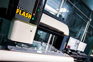
Wafer dimensional capabilities start with the cutting (or Wafer Blank) process but are ultimately determined by the CNC Edging process. Standard Dimensional Tolerance is +/-.2mm and can be held as low as +/-25um if needed. Orientation Notches and Flats are held to SEMI Standard Specifications. Custom features including fiducial marks, cavities, and holes can be applied with positioning tolerances to 25um. All dimensions are verified using an Optical CMM and data can be captured for SPC and COA requirements.
Thickness
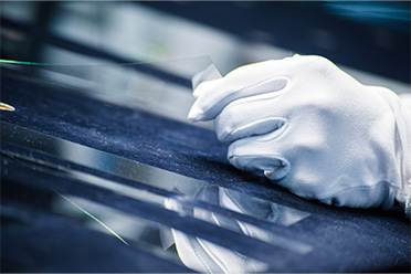
Often, wafer thickness specifications will fall within the glass manufacturers' normal tolerances. When it does not, or when a bulk material (like Fused Silica or Optical Glass) is needed, Coresix can double-side lap wafers to very precise thicknesses and tolerances. Though final specifications are determined through subsequent polishing processes, thickness (as well as flatness and parallelism) are established at this stage. Ultimately, we can achieve thickness tolerances to +/-5um with variation within the wafer to <2um.
Flatness
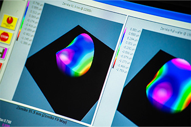
There are many ways to express wafer flatness requirements including Bow & Warp, TIR, P-V, Wave, Fringes, Astigmatism, Power, and Irregularity, etc. We speak the many languages of wafer flatness and can provide the specifications you need with the measurements to validate. Through precision Double-Side Lapping and Polishing processes, we can meet the most stringent of flatness needs demands for today’s technologies.

Parallelism
Whether expressed in Arc Seconds, microns of Thickness Variation (TTV) or Transmitted Wavefront Error (TWE), our processes can create near-perfect parallelism between the two wafer surfaces. Enabling a high level of alignment accuracy in the wafer bonding process, we can produce and verify wafers to your most demanding requirements. We commonly achieve thickness variations levels less than a single micron level.
Roughness
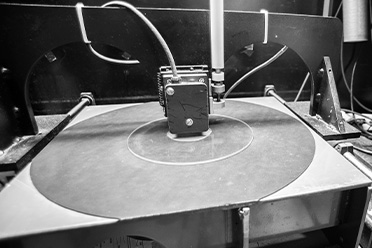
Where surface roughness is a factor, our standard polishing process results in an average roughness between 4A and 7A. For critical surface roughness requirements, Coresix has developed a “Super Polish” process achieving surfaces to 2A Ra, virtually eliminating any trace of subsurface damage.
Cosmetic
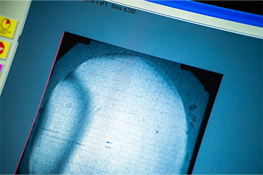
Surface quality levels can be specified in many ways including the common “Scratch and Dig” standards, Maximum Defect Size, Light Condition (under which no visible defect is permissible), etc. Though polishing is often the final step in producing low defect wafers, it is the focus of our entire process to minimize defects through handling practices and process design. We regularly produce wafers to a 5/1 scratch and dig specification.

Cleaning
Wafer cleanliness is a key concern for most wafer coating and packaging applications. Coresix has multiple ultrasonic cleaning lines feeding into a Class 100 Optical Clean Room. In addition to glass surface imperfections, we are inspecting for residue and particulate. This is a secondary inspection under a high-intensity light designed to enable the inspector to detect any level of cleanliness issue. Regardless of the terminology used to specify the wafer cleanliness, we work closely with our customers to assure what they are receiving exceeds their cleanliness expectations.
Inspection
With highly experienced operators in a Class 100 Optical Clean Room, Coresix can accurately and consistently verify the pristine surface conditions we create in our process. By using an appropriate light source, specifically calibrated for the surface condition to which we are inspecting, we can establish spec limitations to the highest standards and meet them reliably in high volume production.

Packaging
Coresix stocks Entegris and Epak semiconductor shipping containers for all standard wafer formats. We also have creative solutions for non-standard wafer dimensions. Once cleaned through our ultrasonic lines and inspected in our Class 100 Optical Clean Room, wafers are packed in an appropriate shipping container, double bagged, vacuum sealed and delivered in a cleanroom ready condition.
Laser Marking
With both UV and CO2 systems, Coresix can effectively mark nearly any glass composition. For OCR applications, our marking is calibrated to provide chip-free, high contrast characters on the surface of the glass. With the UV Laser Systems, we can also apply markings below the surface. Our custom software can accommodate the most complex sequencing, including checksums, while assuring against duplication. Coresix can provide complete traceability and metrology for each individual part.